Skip to content
judahjzndr.blogofoto.com
Welcome to our Blog!
No posts yet
1
2
3
4
5
6
7
8
9
10
11
12
13
14
15
Celebrity Then and Now
Emilio Estevez Then & Now!
Haley Joel Osment Then & Now!
Mr. T Then & Now!
Barbi Benton Then & Now!
Traci Lords Then & Now!
Search for:
Links
Log in
Homepage
Start page
Start your own blog
Start your own blog
Report this page
Archives
2025
Categories
Blog
Meta
Log in
Entries
RSS
Comments
RSS
WordPress.org
1
2
3
4
5
forum
 Emilio Estevez Then & Now!
 Haley Joel Osment Then & Now!
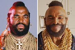 Mr. T Then & Now!
 Barbi Benton Then & Now!
 Traci Lords Then & Now!